- 您现在的位置:买卖IC网 > Sheet目录512 > SI6413DQ-T1-E3 (Vishay Siliconix)MOSFET P-CH 20V 7.2A 8TSSOP
Si6413DQ
Vishay Siliconix
P-Channel 1.8-V (G-S) MOSFET
PRODUCT SUMMARY
FEATURES
V DS (V)
- 20
R DS(on) ( Ω )
0.010 at V GS = - 4.5 V
0.013 at V GS = - 2.5 V
0.016 at V GS = - 1.8 V
I D (A)
- 8.8
- 7.6
- 6.8
? Halogen-free
? TrenchFET ? Power MOSFET
APPLICATIONS
? Load Switch
RoHS
COMPLIANT
? PA Switch
? Charger Switch
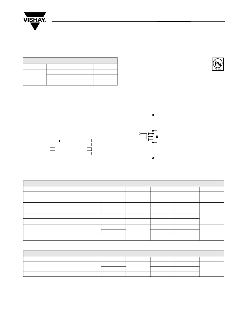
S*
TSSOP-8
G
* Source Pins 2, 3, 6 and 7
D
1
8 D
must be tied common.
S
S
G
2
3
4
Si6413DQ
7 S
6 S
5 D
Top View
Ordering Information: Si6413DQ-T1-GE3 (Lead (Pb)-free and Halogen-free)
D
P-Channel MOSFET
ABSOLUTE MAXIMUM RATINGS T A = 25 °C, unless otherwise noted
Parameter
Drain-Source Voltage
Gate-Source Voltage
Symbol
V DS
V GS
10 s
Steady State
- 20
±8
Unit
V
Continuous Drain Current (T J = 150 °C) a
Pulsed Drain Current (10 μs Pulse Width)
T A = 25 °C
T A = 70 °C
I D
I DM
- 8.8
- 7.0
- 30
- 7.2
- 5.7
A
Continuous Source Current (Diode Conduction) a
I S
- 1.35
- 0.95
Maximum Power Dissipation a
Operating Junction and Storage Temperature Range
T A = 25 °C
T A = 70 °C
P D
T J , T stg
1.5
1.0
- 55 to 150
1.05
0.67
W
°C
THERMAL RESISTANCE RATINGS
Parameter
Symbol
Typical
Maximum
Unit
Maximum Junction-to-Ambient a
Maximum Junction-to-Foot
t ≤ 10 s
Steady State
Steady State
R thJA
R thJF
60
100
35
83
120
45
°C/W
Notes:
a. Surface Mounted on 1" x 1" FR4 board.
Document Number: 72084
S-80682-Rev. B, 31-Mar-08
www.vishay.com
1
发布紧急采购,3分钟左右您将得到回复。
相关PDF资料
SI6423DQ-T1-GE3
MOSFET P-CH 12V 8.2A 8-TSSOP
SI6466ADQ-T1-GE3
MOSFET N-CH 20V 6.8A 8TSSOP
SI6467BDQ-T1-GE3
MOSFET P-CH 12V 6.8A 8TSSOP
SI6924AEDQ-T1-GE3
MOSFET N-CH 28V ESD 8-TSSOP
SI6926ADQ-T1-GE3
MOSFET DL N-CH 20V 4.5A 8-TSSOP
SI6928DQ-T1-GE3
MOSFET DL N-CH 30V 4A 8-TSSOP
SI6933DQ-T1-GE3
MOSFET P-CH D-S 30V 8-TSSOP
SI6955ADQ-T1-GE3
MOSFET P-CH D-S 30V 8-TSSOP
相关代理商/技术参数
SI6413DQ-T1-GE3
功能描述:MOSFET 20V 8.8A 1.5W 10mohm @ 4.5V RoHS:否 制造商:STMicroelectronics 晶体管极性:N-Channel 汲极/源极击穿电压:650 V 闸/源击穿电压:25 V 漏极连续电流:130 A 电阻汲极/源极 RDS(导通):0.014 Ohms 配置:Single 最大工作温度: 安装风格:Through Hole 封装 / 箱体:Max247 封装:Tube
SI6415DQ
功能描述:MOSFET 30V/25V PCh MOSFET RoHS:否 制造商:STMicroelectronics 晶体管极性:N-Channel 汲极/源极击穿电压:650 V 闸/源击穿电压:25 V 漏极连续电流:130 A 电阻汲极/源极 RDS(导通):0.014 Ohms 配置:Single 最大工作温度: 安装风格:Through Hole 封装 / 箱体:Max247 封装:Tube
SI6415DQ-T1
功能描述:MOSFET 30V 6.5A 1.5W RoHS:否 制造商:STMicroelectronics 晶体管极性:N-Channel 汲极/源极击穿电压:650 V 闸/源击穿电压:25 V 漏极连续电流:130 A 电阻汲极/源极 RDS(导通):0.014 Ohms 配置:Single 最大工作温度: 安装风格:Through Hole 封装 / 箱体:Max247 封装:Tube
SI6415DQ-T1-E3
功能描述:MOSFET 30V 6.5A 1.5W RoHS:否 制造商:STMicroelectronics 晶体管极性:N-Channel 汲极/源极击穿电压:650 V 闸/源击穿电压:25 V 漏极连续电流:130 A 电阻汲极/源极 RDS(导通):0.014 Ohms 配置:Single 最大工作温度: 安装风格:Through Hole 封装 / 箱体:Max247 封装:Tube
SI6415DQ-T1-GE3
功能描述:MOSFET 30V 6.5A 1.5W 19mohm @ 10V RoHS:否 制造商:STMicroelectronics 晶体管极性:N-Channel 汲极/源极击穿电压:650 V 闸/源击穿电压:25 V 漏极连续电流:130 A 电阻汲极/源极 RDS(导通):0.014 Ohms 配置:Single 最大工作温度: 安装风格:Through Hole 封装 / 箱体:Max247 封装:Tube
SI6421DQ
制造商:VISHAY 制造商全称:Vishay Siliconix 功能描述:P-Channel 12-V (D-S) MOSFET
SI6423DQ
制造商:VISHAY 制造商全称:Vishay Siliconix 功能描述:P-Channel 12-V (D-S) MOSFET
SI6423DQ_05
制造商:VISHAY 制造商全称:Vishay Siliconix 功能描述:P-Channel 12-V (D-S) MOSFET
